Isolated Gate Driver PCB For (high side) MOSFET Switching
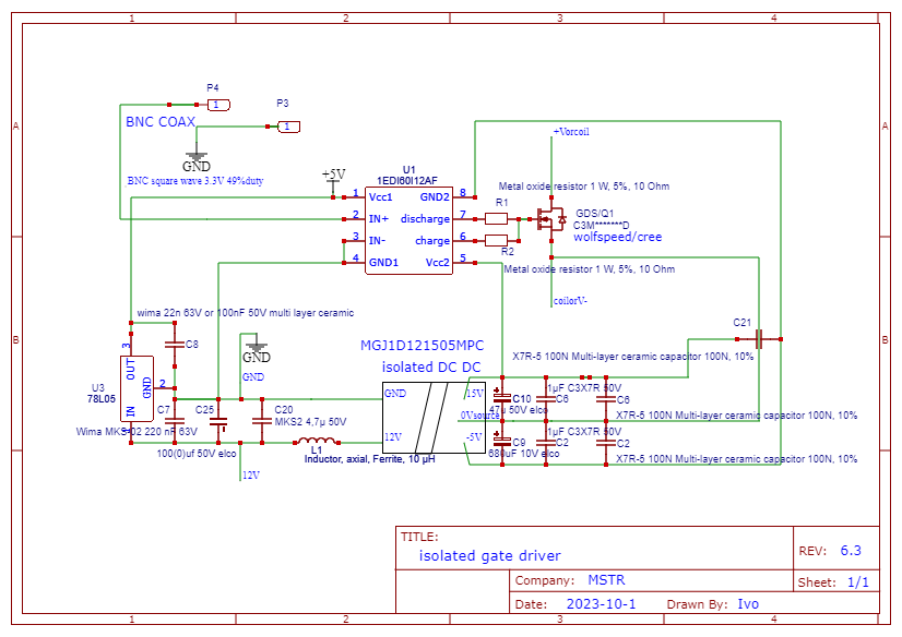
The MOSFET is the best choice for fast switching a coil on and off. Above picture is the schematic. My current design has one driver per pcb for one MOSFET.
The isolated MOSFET gate driver PCB can be used for:
– Half bridge switching
– H bridge switching
– high- and low side switching
– series- and or parallel switching
I have designed the mosfet switch as a single PCB, which is able to switch a single MOSFET.
When 2 or 3 PCBs are hooked up in series, much higher switching voltages can be achieved.
The PCB’s can also be used in parallel, for high current capabilities.
And even in series parallel for combined high voltage and high current.
For best results, Vth (threshold voltage) of Gate-Source, must be matched within 10% for all MOSFETS
The voltages are not only limited by the MOSFET(s),
But also by the isolated gate driver and the isolated DC to DC converter. which are rated at 5kV.
The MOSFET switch pcb gerber file and the BOM (Bill of materials) can be downloaded here (click orange buttons).
The zip file can be directly uploaded to the JLCPCB.com order page. And the BOM has links to order the parts needed.
Be aware that this MOSFET switch PCB is the heart of the circuit,
but at least needs an external 12v dc power supply and a square wave signal generator to function.
I have designed it to have a 12V power input, for the gate driver circuit,
and an extra separate power supply for the MOSFET switch (where the coils can be connected).
*C21 is connected between pin 5 and 8 of the U1 gate driver IC. it is a 100nF X7R-5 multilayer ceramic capacitor.
This design is shared open source. A donation is appreciated, with this you support my ongoing research into free electricity for all.